Welcome
My name is Markus PRISTOVSEK, I am the head and the only permanent member of the international section. Since almost nobody pronounces my name correctly on the first try, just call me Markus.
Light onto the black art of semiconductor formation
In recent years the growth of nitrides for LEDs used in light bulb, laser diodes, and ultra-violet LEDs for water purification and air disinfection became challenging not only from an academic point of view but from a several billion dollar industrial perspective. The workhorse for the production of the layer structures is the so-called metal-organic vapour phase epitaxy (MOVPE). Now even politicians come to start up a new MOVPE: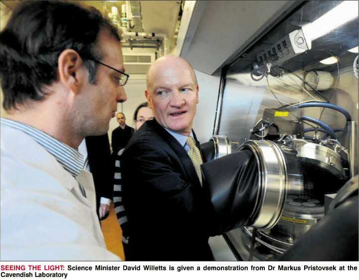 The photo on the right shows a younger me (to the left) with the then British Science Minister David Willets at the opening of the new 6×2 MOVPE reactor at the Cavendish laboratory of Cambridge University in 2013.
Apart from LEDs, you have also some of the latest results of III-nitride research in your pocket. The high-frequency chip creating the radio signals and which hooks you up to the wireless network is almost certainly a GaN-based "high electron mobility transistor", short HEMT. GaN-based HEMTs have very high efficiency at high frequencies. For a similar reason, HEMTs have enabled the recent shrinking of chargers and power supply while increasing their efficiency.
Due to the importance of GaN, large efforts are devoted worldwide into research of nitride semiconductor growth and device development. Even though, growth by MOVPE is done in hundreds of laboratories and factories worldwide, it is not very well understood. Brute force optimisation lead to the nanostructures used in current devices (which are often less than 10 atoms in height). Further progress needs finer control of unwanted defects (like carbon, or missing atoms) below the 1/billion level, especially of one wants devices that can handle high voltage directly without the need of transformers.
As a small university group, it is important to try approaches not possible in an industrial environment. Hence, we focus on new materials or orientations to enable new electronic or optical devices. And even then, a big task is easier with collaboration. We are very closely related to the Amano-lab and had and have international visiting students from France, Italy, and Germany, and we collaborate with groups in Germany, Singapore, Ireland, and China.
About myself
I started studying basic physics at the Technical University of Berlin in 1989, weeks before the Berlin Wall came down. In 1995, I obtained my Diploma(Master) at Prof. Richter’s Group about Growth and Passivation of III-V-Semiconductors. The group was the leading group to build and use Reflectance Anisotropy Spectroscopy (RAS) to study cubic III-V semiconductor growth in metal-organic vapor phase epitaxy, the workhorse of III-V semiconductor nanostructure growth till this day. I completed my PhD in the same group in 2000. Our research and development of in-situ monitoring was quite successful and led to the foundation of the company LayTec which is still thriving today. Not least because modern semiconductor growth requires good in-situ monitoring for success.
But when LayTech was founded, I decided to pursue instead an academic career and followed an offer that I had recieved from the National Institute for Materials Science in Tsukuba, Japan on in-situ characterisation by RAS combined with in-situ Scanning Tunneling Microscopy (STM). The latter allows in principle to follow the growth atom by atom as they arrive and move on the surface.
Back in Berlin, after a short stay at the Ferdinand-Braun-Institut für Höchstfrequenztechnik I joined again the Technical University of Berlin as Assitant, where I led the MOVPE activities. New materials such as InN and novel ferromagnetic semiconductors like InAsP:Mn with a tailorable Mn acceptor depth were investigated, with the main focus on the growth process. A very special result was the first and only in-situ STM for MOVPE. This has been the only STM worldwide that could operate at 700°C at near atmospheric pressure. Other innovative tools were the only multi-channel RAS setup for semiconductor epitaxy, and three spectroscopic ellipsometers for during growth studies. These were put to use to measure unknown refractive indices at high temperature, to study surfaces (especially of nitride semiconductors), and to learn about the relaxation of In containing alloys. So, over the years my research focus changed from GaAs and related towards the III-nitride semiconductors. This materials system is strongly driven by industrial application like LEDs and now HEMTs, so there are still many open questions and sideways no covered. After nearly ten years in Berlin, I joined the GaN center at Cambridge University (UK) in 2012 as Senior Researcher, focussing on long wavelength InGaN LEDs. Our hope was with the (11-22) crystal orientation, which is called semi-polar, because it is between the polar (0001) and the non-polar (1-100) orientation. Polar refers to the internal polarisation, which arises from a charge transfer between the alternating nitrogen and metal atomic layers. Since the LEDs did not show the expected performance, I delved into finding out why. That took many year, but finally we could show that the sign of the polarisation is the key.
Since 2017, I was appointed Designated Professor at Nagoya University (which means that after my retirement, no new professor will be appointed to my position). This is a the newly found Center of Intergrated Research of Future Electronic (CIRFE) at the Institute of Materials and Systems for Sustainability. Hence, my focus is nowadays on electronic devices.
You find more technical data on my profile page at NU which contains list of recent talks, literature, and funding.